Ever wonder what it takes to design a custom core module around the STM32H7A3 for your own project? With so many pins, connectors, and layout decisions, a good schematic review is the best way to catch mistakes before you get to the tricky business of PCB layout—especially if it’s your first board.
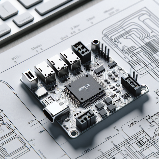
This post takes a close look at a compact STM32H7A3 core module designed for a Formula Student project. The module exposes most of the MCU’s pins through two Hirose DF12NB (3.0 mm) mezzanine connectors and packs in useful on-board features like a microSD slot (1-bit mode) and USB-C Full-Speed support. If you’re about to build your own “core board” or just want ideas on pinout, power, or connector best practices, read on.
Key Features of the STM32H7A3 Core Module
At the heart of this board is the STM32H7A3RGT6, a high-performance ARM Cortex-M7 microcontroller from STMicroelectronics. What makes this particular core module interesting?
- Most MCU pins are broken out to two DF12NB mezzanine connectors (3.0 mm pitch), making it flexible for daughterboards or custom baseboards.
- On-board microSD slot supports 1-bit mode—handy for logging or configuration data.
- USB-C Full-Speed interface (with proper orientation handling).
- Designed as a 4-layer PCB to help with signal integrity and power distribution.
For many students or hobbyists, jumping straight into a complex core module like this can feel overwhelming. But with careful planning and a schematic review, you’ll save yourself a ton of debugging time down the road.
Power & Decoupling: How Much is Enough?
One of the biggest challenges on any high-speed MCU board is getting power and decoupling right. On this module, the power supply and decoupling networks follow classic best practices:
- Each VDD pin gets its own decoupling cap (typically 100nF ceramic), placed as close as possible.
- Bulk capacitance is provided near the MCU to handle transients.
- On the microSD interface (1-bit mode), pull-ups are added on CMD/DAT0 lines as per the SD spec.
- A series resistor (“series-termination”) is available on the CLK line to dampen reflections—useful for short runs (under 2-3 cm), but you might be able to skip it for really short traces.
If you’re wondering if your SD pull-ups and series resistor are reasonable for a board like this—the answer is yes! For 1-bit mode and short trace lengths, this setup matches what’s commonly found in official app notes from SD Card Association documents.
USB-C Full-Speed: Handling Orientation and ESD
USB-C may look simple from the outside, but wiring it up takes care. There are two main points to watch:
- CC (Configuration Channel) resistors are required to let a host or device know which way the plug is inserted. For Full-Speed (not Power Delivery), 5.1kΩ pull-downs on CC1/CC2 are typical.
- ESD/TVS diodes protect sensitive MCU pins from electrostatic discharge. Make sure these are placed as close as possible to the connector.
- Double-check your connector footprint—USB-C has more pins than USB Micro-B. Only use the ones needed for Full-Speed data and power.
If you want more details on good USB-C hardware design, check out the Texas Instruments USB Type-C Hardware Design Guidelines.
Mezzanine Connectors: Pinout, GND Returns & Routing Tips
The real challenge with a core module is making sure high-speed signals and sensitive analog lines don’t fight each other across the connectors. The rule of thumb is that roughly 30% of mezzanine connector pins should be ground (GND). This helps maintain low-inductance return paths—crucial for fast digital signals.
But how do you allocate GND pins? Here’s a quick checklist:
- Spread GND pins evenly across both connectors.
- Place GND next to high-speed or noisy signals wherever possible to provide “return highways.”
- If you can spare more than 30% GND pins, do it—especially if you have lots of I/O switching at once.
- Keep power/ground pairs together to limit crosstalk.
When it comes to layout and routing advice, there aren’t a lot of “official” guides targeted at the DF12 series. But the general rules from high-speed design apply:
- Keep signal traces as short and direct as possible.
- Avoid running parallel high-speed traces for long distances across the connector to minimize crosstalk.
- Reference ground planes under critical signals whenever possible.
For more on connector layout in general, Sierra Circuits’ PCB connector guidelines offer some universal tips.
Personal Experience: Why Reviews Matter
When working on my own first STM32-based board, I remember feeling lost over where to put all those decoupling caps—and how many GND pins I should squeeze into my connector footprint. A mentor showed me some teardown photos from production modules. Suddenly it made sense why some designs “waste” so many pins on GND—it saves hours chasing down weird glitches later!
It’s easy to want to maximize I/O count on a small connector, but reliable returns are worth the tradeoff.
Takeaways & Your Next Steps
To wrap up, here’s what matters most when reviewing an STM32H7A3 core module schematic:
- Use plenty of decoupling on every MCU supply pin.
- Add SD pull-ups and consider a CLK series resistor for short runs.
- Handle USB-C orientation with CC resistors and protect data lines with ESD diodes.
- Aim for at least 30% GND allocation in your mezzanine pinout, more if possible.
- Plan signal routing with returns in mind—don’t be afraid to tweak pinout during layout.
Designing your first complex core module is ambitious—but totally doable with careful planning. What layout tricks or review tips have saved you from headaches on your own PCBs?
Leave a Reply