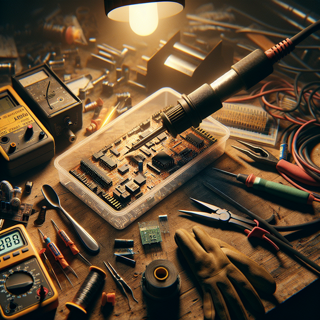
Making a diy pcb sounds tricky until you realize it’s mostly about patience and good lighting. The reason it matters now? Component prices are down, free design tools abound, and small-run prototyping no longer needs a factory. In the next hour you can sketch a working board layout and prep it for etching—no industrial lab required.
Why DIY PCBs Are Having a Moment
Until recently, getting a circuit board meant waiting weeks for an overseas fab house or paying extra for rush service. But hobbyists like Reddit user qucolking show that homemade boards can look pro-grade if you use the right process flow. Between low-cost laser printers and copper-clad boards on Amazon, the barrier has all but vanished. The only real change is mindset—you can iterate faster when you own every step from schematic to solder mask.
Open-source CAD tools such as KiCad and EasyEDA let anyone map traces with grid snapping and design rules built-in. Combine that with cheap ferric chloride or sodium persulfate etchants, and suddenly your kitchen doubles as a mini fab line. Even if you eventually outsource production, learning the manual method teaches how trace widths and pad spacing behave in the real world—something simulators can’t fully convey.
How to Build Your First DIY PCB
The workflow isn’t glamorous—but it’s concrete and repeatable. Do this once carefully and the second run feels routine.
- Step 1 – Design: Open KiCad → “File” → “New Project.” Draw your schematic; assign footprints early so pads match later. Run “Inspect → Design Rules Check” to catch shorts before exporting.
- Step 2 – Print: From the PCB editor choose “Plot.” Set format to PDF or PNG (mirrored). Print on glossy magazine paper with a laser printer; inkjet won’t transfer cleanly.
- Step 3 – Transfer: Place print face-down on copper-clad board. Use an iron set around 180 °C; press evenly for 5–6 minutes. Let cool; soak in warm water; peel gently so toner stays on copper.
- Step 4 – Etch: Mix ferric chloride per label instructions (wear gloves). Agitate tray lightly until exposed copper disappears—usually under 10 minutes. Rinse thoroughly with cold water.
- Step 5 – Drill & Solder: Use a 0.8 mm bit in a Dremel for through‑holes. Clean pads with isopropyl alcohol before soldering components.
Sanity check: after step 4 hold the board up to light; all intended traces should be intact, no hairline bridges between pads. If you see faint copper slivers connecting pads—back into etchant for 30 seconds more.
Anecdote From the Bench
I watched a friend knock out his first board last weekend—a simple LED flasher using a 555 timer. He printed two copies just in case one failed during transfer. The first came out blotchy; the second looked sharp enough to pass factory inspection. His grin said it all when both LEDs blinked in rhythm—proof that household‑grade tools can yield precise geometry when handled deliberately.
The fun part? He immediately spotted layout tweaks he’d never noticed onscreen—the proximity of traces near the IC made him appreciate why clearance rules exist. That tactile feedback turns abstract “design rules” into muscle memory.
Nuance: When Homemade Isn’t Ideal
The contrarian view is that not every project benefits from home‑etched boards. For fine‑pitch microcontrollers or dense multilayer designs, professional fabs win on precision and safety. Ferric chloride stains anything porous—it’ll ruin countertops if spilled—and double‑sided alignment can drift by half a millimeter without registration pins.
The fix is hybrid workflow: prototype single‑sided logic or sensor boards yourself; send complex signal layers to services like JLCPCB. This approach lets you debug low‑speed circuits locally while saving precision work for automated drills and plating baths you can’t replicate at home.
If etchant disposal worries you (and it should), neutralize spent solution with baking soda until fizzing stops before sealing it in waste containers per local e‑waste guidelines—EPA guidance here.
Quick Wins for Cleaner DIY PCBs
- Pre‑heat your board on the iron for 30 seconds before placing toner—helps adhesion.
- Tape edges of paper to keep it from shifting mid‑press.
- If traces lift after etching, patch them with conductive silver pen instead of restarting.
- Use blue painter’s tape around drill zones to reduce copper burrs.
- Label pin numbers directly on silkscreen layer—even Sharpie ink works if sealed later with clear coat.
Troubleshooting Common Gotchas
Toner won’t stick? Likely too little heat or dirty copper. Scuff lightly with 1000‑grit sandpaper until shiny before retrying transfer.
Pads missing after etch? Over‑etched board; shorten bath time or mix fresher solution.
Solder bridges? Reduce tip temperature below 350 °C and use flux liberally; drag tip across pins horizontally rather than dot by dot.
No continuity? Use multimeter’s beep mode after drilling; sometimes microcracks hide under varnish layers.
You’ll quickly learn to read visual cues—the color of etched copper shifts slightly before full removal, like bronze fading to dull pink—that’s your sign to rinse immediately.
The Payoff
The biggest upside isn’t saving money—it’s control over iteration speed. You burn an hour making mistakes that would otherwise take days via shipping delays. More importantly, each misprint trains your eye toward manufacturability—trace angles under 45°, avoiding acute intersections that trap etchant bubbles. That intuition carries straight into professional CAD work later on.
A subtle gain is confidence in analog layouts. When routing op-amp stages or sensor interfaces by hand, you start thinking about current loops physically instead of numerically—a trait veteran engineers swear by but rarely teach formally.
The Bigger Picture of DIY Fabrication
This resurgence of bench-level making mirrors what software devs did decades ago with open compilers—the tooling democratized creativity. With cheap laser cutters and small CNC routers joining the mix, home labs blur lines between electronics and mechanics again. Once you’ve made your own board successfully, designing enclosures or integrating sensors becomes less theoretical—you already trust your hands more than datasheets alone.
If there’s any myth worth breaking, it’s that professional finish equals expensive gear. Consistent process beats fancy tools nine times out of ten. Keep logs of temperature settings and timing; treat each run like lab data rather than art project—that’s how repeatability sneaks in quietly.
Your Turn
You’ve seen how manageable this process really is—from toner transfer to drilling holes that actually line up with headers. So what circuit will earn its copper tonight—a sensor breakout or maybe a small synth voice? Either way, start small but record everything; future-you will thank present-you when scaling up becomes just another controlled experiment.
Leave a Reply